
Abstract
This paper describes a general approach for transferring clean single-layer graphene onto silicon nitride nanopore devices and the use of the electron beam of a transmission electron microscope (TEM) to drill size-controlled nanopores in freely suspended graphene. Besides nanopore drilling, we also used the TEM to heal and completely close the unwanted secondary holes formed by electron beam damage during the drilling process. We demonstrate electron beam assisted shrinking of irregularly shaped 40–60 nm pores down to 2 nm, exhibiting an exquisite control of graphene nanopore diameter. Our fabrication workflow also rendered graphene nanopores hydrophilic, allowing easy wetting and use of the pores for studying protein translocation and protein–protein interaction with a high signal to noise ratio.
Export citation and abstract BibTeX RIS
It has been established that the thickness of the insulating membrane significantly affects the signal to noise ratio (SNR) [1] and spatial resolution [2, 3] in nanopore sensors. Attempts to develop high-resolution resistive pulse sensors for DNA sequencing has encouraged the use of single or multilayer graphene in nanopore devices [4–9]. The thickness of single-layer graphene is commensurate with the base stacking distance along the DNA backbone, making it an ideal membrane for high-resolution DNA analysis using solid-state nanopores [4]. Moreover, low-aspect-ratio graphene pores can be used for high-resolution probing of proteins, where they can enable detection of conformational changes and protein–protein interactions at the single-molecule level [10]. However, since the first use of graphene for nanopore devices in 2010, only a handful of reports have been published and the potential of graphene nanopores for single-molecule DNA and protein sensing has not been fully realized. This is due to the challenges associated with fabrication of functional graphene pores. The ability to produce graphene nanopore devices capable of analyte detection is limited by the strategies for transferring clean and defect-free graphene and fabricating nanopores of the desired shape and dimensions in the suspended graphene membrane and by the inherent hydrophobicity of graphene, which prevents molecular translocation through the pore.
Fabrication of graphene nanopores is a complex, labor-intensive and time-consuming process with multiple failure modes. The challenges associated with the individual steps result in a high failure rate, and new researchers face significant barriers upon entering the field. Some process improvements for individual steps have been demonstrated in the materials science literature; however, a comprehensive account of the complete fabrication process is missing; through this report we try to bridge this gap. Most graphene transfer recipes start with coating the graphene surface with a polymer layer (such as polymethylmethacrylate, PMMA), which protects the graphene and serves as a mechanical support during the transfer process. After the transfer is complete, the polymer is dissolved using acetone or another solvent; however, these solvents fail to completely remove PMMA, resulting in dirty membranes with large patches of support polymer remaining [11–13]. Several different polymers [14–16] and cleaning strategies [4, 13, 14] have been employed to minimize polymer residues on the graphene surface after the transfer. In comparison with solvent cleaning, thermal annealing in a gaseous atmosphere [13, 17–19] or a vacuum [20] has been particularly useful in removing residual PMMA and has been shown to produce very clean graphene membranes. Even when nearly complete removal of PMMA from the graphene surface can be achieved; drilling nanopores in the extremely thin graphene using the high-energy electron beam of a transmission electron microscope (TEM), often results in the formation of over-sized pores. In the few journal articles published on graphene nanopores, problems such as pinholes [5], secondary holes, irregularly shaped pores [8] and complete membrane damage [9] during TEM drilling of graphene have been routinely reported (see online supplementary figure S3 for examples of such defects). The challenge is further complicated by the hydrophobicity of graphene, which prevents membrane wetting and consequently the translocation of analyte molecules, thereby rendering graphene pores unusable.
In this paper we report an optimized approach to the fabrication of graphene nanopores and address challenges associated with each fabrication step. The general approach presented here can be used to easily produce functional graphene pores capable of analyte detection. We demonstrate transfer of clean single-layer graphene onto pre-drilled SiO2/SixNy pores and fabrication of size-controlled nanopores in a suspended graphene membrane by electron beam assisted drilling and shrinking. We also show that the electron beam can be used to heal pinholes or any unwanted secondary holes formed during the pore drilling step. Our fabrication workflow also results in a naturally hydrophilic graphene surface, which facilitates pore wetting and analyte translocation. We demonstrate the use of our pores for investigation of single protein translocations and protein–protein complex formation with a high SNR. The experimental approach outlined in this paper can improve the fabrication yield of graphene nanopore devices and enable researchers to carry out single-molecule studies using extremely thin nanopores.
Results and discussion
Graphene transfer process
For the preparation of graphene nanopore devices, graphene grown by chemical vapor deposition (CVD) was transferred onto pre-drilled SiO2/SixNy pores using published recipes [6, 7] with modifications (figure 1). We started with drilling 500 nm diameter pores in free-standing silicon nitride membranes (50 nm thick) using a focused ion beam (FIB; FEI Strata DB 235 FIB) as described earlier [21, 22]. The chips with pores were then coated with a 100 nm thick layer of silicon dioxide on either side using pressure-enhanced CVD (PECVD). These SiO2/SixNy pores served as the receiving substrates onto which graphene was transferred (see below). CVD grown graphene (on Cu/SiO2/Si) was spin-coated (3000 rpm for 30 s) with 1% PMMA prepared in chlorobenzene. The silicon wafer was cut into 3 mm × 3 mm pieces and the SiO2 layer was etched using 7:1 buffered oxide etch (J.T. Baker) for 1 h. During this 1 h etching process, etchant eroded the SiO2 layer from all sides, while the graphene remained safely sandwiched between the PMMA and copper layers. Etching of the SiO2 released a PMMA/graphene/Cu multilayer structure floating in buffered oxide etch (BOE). After three quick washes in deionized water, the copper layer was etched in ammonium persulfate (APS Copper Etch 100, Transene Company Inc., Danvers, MA, USA) solution for 10 min, leaving PMMA/graphene layers floating on APS. Some protocols directly etch the copper layer from PMMA/graphene/Cu/Si or PMMA/graphene/Cu/SiO2/Si multilayer constructs by incubating them in APS for 30 min to 1 h. However, in the direct etching method the graphene layer is also exposed to APS after the copper layer has been etched away, causing chemical insult to the graphene membrane. The sequential etching of SiO2 and copper in our protocol minimized chemical damage to the graphene during the copper etching process since the copper was exposed to APS for only 10 min. Following copper etching, PMMA/graphene layers were washed three times in deionized water and were scooped and transferred onto SiO2/SixNy nanopore chips. The nanopore chips with PMMA/graphene were placed on a hot plate at an angle of 45° and dried (figure 2). Finally, PMMA was removed by two-step thermal annealing in ambient air using a Thermolyne (Thermo Fisher Scientific) benchtop muffle furnace. We heated the chips at 180 °C for 30 min followed by 400 °C for 2.5 h (see the following section for detailed reasoning).

Figure 1. Process flow for graphene transfer and fabrication of graphene nanopores. (a) A 500 nm pore was drilled in a free-standing silicon nitride membrane using a FIB. (b) A 100 nm layer of silicon dioxide was deposited on either side of the chip using PECVD. (c) SiO2 was etched for 1 h from the PMMA/graphene/Cu/SiO2/Si multilayer structure using 7:1 buffered oxide etch. (d) Copper was etched for 10 min from PMMA/graphene/Cu using ammonium persulfate at room temperature. (e) The PMMA/graphene layer was transferred over the nanopore chip prepared in step (b). (f) Chips were dried at an angle of 45° to achieve asymmetric drying in order to get rid of any residues left behind by evaporating water. (g) PMMA was removed by thermal annealing in ambient air at 180 °C for 30 min followed by 400 °C for 2.5 h. (h) The desired nanopore was then fabricated in the suspended graphene membrane using electron beam assisted drilling and shrinking.
Download figure:
Standard image High-resolution image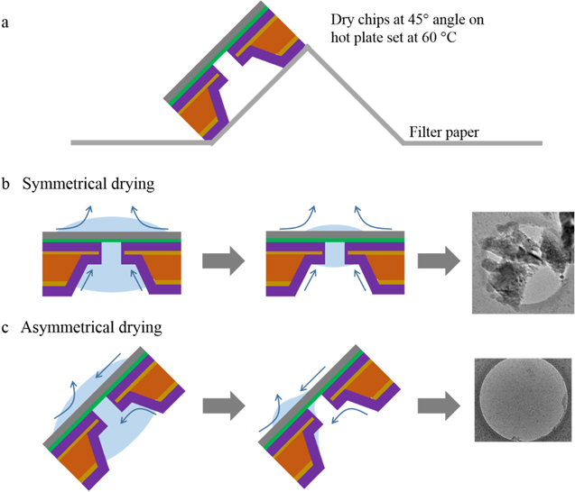
Figure 2. Effect of symmetrical and asymmetrical drying on the quality of the transfer process. (a) After scooping PMMA/graphene from water onto nanopore chips, the chips were dried by placing them on a filter paper at an angle of 45°. The filter paper was placed on a hot plate maintained at 60 °C. (b) Placing the chips flat on the surface results in symmetrical drying of water from the chips. Since the etch pit and nanopore are in the center of the chip, symmetrical drying results in deposition of contaminants on the suspended graphene by evaporating water. (c) Placing the chips at an angle while drying makes the chips dry asymmetrically. The receding water meniscus leaves no contaminants in the central region of the chip, resulting in clean suspended graphene membranes.
Download figure:
Standard image High-resolution imageProcess improvements to produce clean free-standing graphene
In our graphene transfer process, two steps were critical for obtaining a very clean graphene surface: (a) asymmetrical drying of chips after transferring PMMA/graphene onto SiO2/SixNy pores and (b) removal of PMMA from the graphene surface using thermal annealing. Figure 2 summarizes the effect of the drying angle after transferring graphene on SiO2/SixNy pores. The final step (figure 1(e)) of the graphene transfer process is routinely carried out in deionized water. Nominally, this process results in water getting trapped in the etch pits of the nanopore chips. If the chips were dried flat on a surface, symmetrical evaporation of water left residues focused in the free-standing graphene area, resulting in dirty membranes (figure 2(b)). Placing the chips at an angle of 45° on a hot plate lead to asymmetrical drying, in which the water meniscus moved from the top edge of the graphene to the bottom edge, leaving no residues in the central area where the graphene membrane is suspended (figure 2(c)). Figures 2(b) and (c) also show low-resolution TEM images of 500 nm SiO2/SixNy pores with graphene suspended on them. In the case of symmetrical drying, significant residues were seen in the graphene area. Whereas upon drying the chips asymmetrically very clean graphene was obtained. The strategy of drying substrates at an angle of 45° after the graphene transfer process is particularly helpful when transferring graphene to nanopore devices, since water becomes easily trapped inside the etch pit in silicon. The other critical step for obtaining clean graphene is the removal of PMMA by thermal annealing. We performed thermal treatment in a two-step fashion in ambient air. The first annealing step was designed to remove any folds or strain from the transferred membrane and bring it into conformal contact with the flat surface of the receiving substrate. For the first step, an annealing temperature of 180 °C was maintained for 30 min, which melted the PMMA polymer layer (PMMA melting point = 160 °C) and relaxed the graphene membrane. The second annealing step was designed to boil and completely remove PMMA (PMMA boiling point = 200 °C) from the graphene surface. For the second step, surfaces were annealed at 400 °C for 2.5 h. The chips were placed at an angle of 45° inside the furnace during the thermal annealing process so that no residue was left in the center of the suspended graphene membrane when the PMMA was boiled away.
Figure 3(a) shows a low-resolution TEM image of a 500 nm SiO2/SixNy pore with graphene suspended over it. The box marked in red in figure 3(a) is shown at a higher magnification in figure 3(b). The red circle in figure 3(b) was used to collect the specific area electron diffraction (SAED) pattern for the graphene shown in figure 3(c). The characteristic diffraction pattern for graphene with hexagonal symmetry was obtained from our transferred graphene membranes. The SAED image was inverted (converted into a negative image) using ImageJ for better representation. The inset shows the inverse intensity plot for the diffraction spots marked by the red rectangle in figure 3(c). The high SNR seen in the inverse intensity plot indicates the presence of clean and crystalline graphene without significant PMMA (amorphous) residues. The intensity ratio between the first and the second nearest diffraction spots in the SAED pattern can be used to determine the number of graphene layers [23]. As seen in the plot, the intensities of the first spots ( are greater than those of the second spots (
 indicating that the suspended membrane was single-layer graphene.
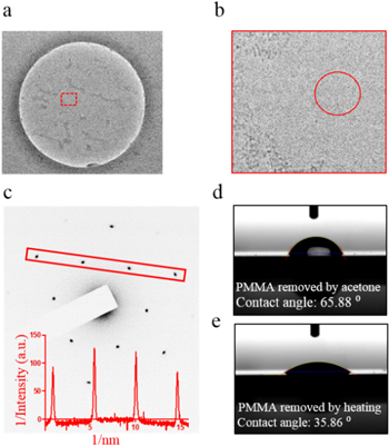
Figure 3. (a) TEM image of freely suspended graphene over a 500 nm diameter pore. (b) Magnified TEM image of the area enclosed in the red square in (a). (c) The SAED pattern shows hexagonal symmetry characteristic of graphene (the SAED pattern was obtained from area marked with red circle in (b)). The SAED image was inverted in ImageJ. The inset shows inverse intensity profiles of diffraction spots enclosed in the red rectangle in the SAED pattern. An intensity ratio greater than one for the first spots compared with the second spots suggests that the graphene is single layer [23]. (d), (e) Contact angle measurement for the graphene surface when PMMA was removed using acetone and by thermal annealing (in ambient air), respectively. Thermal annealing resulted in much cleaner and a hydrophilic graphene surface.
Download figure:
Standard image High-resolution imageImproving the wettability of graphene nanopore devices to enable analyte detection
The hydrophobicity of graphene has proved to be a major impediment to using graphene nanopores for analyte translocation. This has prevented the optimal use of graphene nanopores for DNA and protein analysis. The problem of hydrophobicity of solid-state surfaces is routinely addressed by treating them with air/oxygen plasma; however, plasma treatment etches away graphene layers [24] and results in leaky membranes [9]. Several strategies have been adopted to improve the wettability of graphene nanopores, such as flushing the pores with ethanol [4], atomic layer deposition of titanium dioxide [5] and chemical passivation using amphiphilic molecules [9, 25]. While coating with TiO2 can provide a stable solution to improve the wettability of graphene, the process of using ethanol to make bare graphene pores hydrophilic is usually reversible. The strategies to chemically passivate graphene surface have also met with only moderate success. Shan et al reported that no protein translocations could be detected when graphene nanopores were passivated using mercaptohexadecanoic acid (or C16) and only ferritin (and no bovine serum albumin) translocations could be detected when pores were functionalized with phospholipid–polyethylene glycol (DPPE-PEG750) [9]. Schneider et al reported a reduction in nanopore fouling and more stable recording of DNA translocations when the graphene surface was passivated by the amphiphilic product of reaction between 1-aminopyrine and a N-hydroxysuccinimide ester derivative of a 4-mer ethylene glycol [25]. However, from the data presented by Schneider et al it appears that their chemical functionalization significantly increases the baseline noise, resulting in a low SNR [6, 25]. For double-stranded DNA translocations, a higher SNR has been obtained by using a 22 nm uncoated pore (figure 4(a) in Schneider et al [6]), compared with a 10 nm chemically coated pore (figure 4(a) in Schneider et al [25]). Based on these reports, we believe that chemical passivation is not the optimal solution for graphene hydrophobicity. Other methods need to be employed to improve graphene surface properties to achieve analyte translocation.
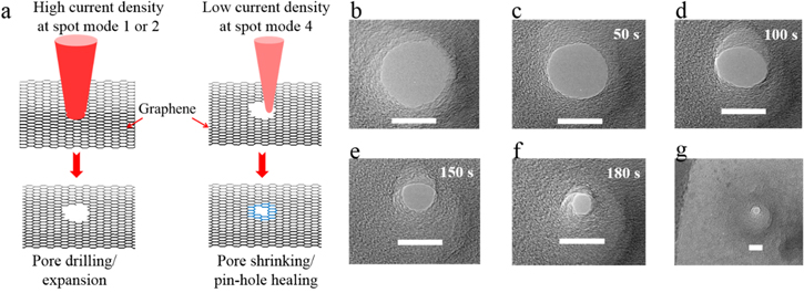
Figure 4. (a) Graphene drilling and shrinking scheme. A high current density electron beam at spot modes 1 and 2 was used to easily drill and expand the nanopores in graphene. When the drilled pores were exposed to a low current density beam at spot modes 3 or 4, the pores could be shrunk down to the desired size. The same process was also used to heal any unwanted secondary pores. (b)–(f) Evolution of shrinking nanopore under low current density electron beam exposure (spot mode 3, TEM at 120 keV). (g) Low-magnification view of the nanopore shrunk in (b)–(f). All scale bars: 15 nm.
Download figure:
Standard image High-resolution imageIn our process flow, the thermal annealing method used for removing PMMA from the graphene surface also resulted in naturally hydrophilic graphene. As shown in figures 3(d) and (e), our graphene samples exhibited a significantly lower water contact angle after thermal annealing (35.86°) compared with the samples for which PMMA was removed by dissolution in acetone (65.88°). For contact angle measurements, graphene/PMMA was transferred to SiO2/Si substrates and PMMA was either removed using thermal treatment (as discussed in the previous section) or acetone (see supplementary figure S2 for an optical image of transferred graphene on a SiO2/Si substrate). Recently it has been demonstrated that hydrophilicity of graphene can be improved by thermal annealing at 300 °C in ∼0.15 l min−1 flow of O2/Ar (1:2) for 2 h, in order to use graphene as an ultrathin TEM sample support [26]. The authors reported that thermal annealing only resulted in minimal structural changes in graphene as revealed by Raman spectra [26]. In our experiments, similar results were obtained by thermal annealing of PMMA at 400 °C for 2.5 h in ambient air.
Thermal annealing significantly lowered the water contact angle for our transferred graphene; however, this alone was not sufficient to produce graphene nanopore devices capable of analyte translocation. Another critical step to produce functional pores was coating of the silicon nitride pore with silicon dioxide before transferring the graphene (figure 1(b)). We had started out with graphene transferred on FIB drilled pores in bare silicon nitride membranes, and our attempts to use such graphene nanopores for analyte detection were unsuccessful. We observed little or no conductance through the pores despite the low water contact angle observed after thermal annealing. The pore behavior was very similar to what we had experienced in the past with hydrophobic silicon nitride pores. For silicon nitride pores, the problem of hydrophobicity was routinely solved by plasma treating the chips for 2–3 min before use. However, we could not plasma treat the chips with a graphene membrane on them, as plasma etches away graphene and would have caused defects in the membrane [9]. We hypothesized that although graphene was hydrophilic (after thermal annealing), the hydrophobic nature of silicon nitride was preventing adequate chip wetting and ionic conduction through the pore. We needed a strategy to make silicon nitride hydrophilic without affecting the graphene membrane sitting on it. We attempted to thoroughly plasma treat the silicon nitride pore before graphene transfer; however, graphene transfer, PMMA removal and nanopore drilling in graphene takes a good amount of time. Within this time, silicon nitride reverts to the hydrophobic form. To address this issue, we coated the silicon nitride pore with 100 nm SiO2 on either side before the graphene transfer process (figure 1(b)). A SiO2 layer on silicon nitride pores made them permanently hydrophilic (see online supplementary figure S1 for contact angle comparison of bare SixNy and SixNy coated with SiO2) and it combined with the hydrophilic graphene membrane, resulted in fully functional graphene nanopores. These pores did not need any further surface treatment and were able to conduct ionic current immediately after assembly into the flow cell.
Graphene nanopore drilling and shrinking
As we mentioned earlier, the fabrication of graphene nanopores is a complex process, and nanopore drilling in suspended graphene membrane is one of the major failure modes. After successful transfer of graphene onto SiO2/SixNy pores, nanoscale pores are typically drilled in the suspended graphene using the electron beam of a TEM. When the high-energy electron beam of a TEM interacts with atomically thin graphene, carbon atoms are knocked out of the plane, resulting in membrane defects. If the electron beam is focused on a specific area of graphene, these atomic defects can grow and combine to form a nanopore. The minimum incident electron energy for knocking in-lattice carbon atoms out of the graphene plane is estimated to be around 86 keV [27], and 80 keV electrons are routinely used to prevent beam damage to graphene. However, nanopores can be efficiently sculpted in graphene by using electron energies above 140 keV [28]. Unfortunately, this pore drilling process is difficult to control and usually results in over-sized irregularly shaped pores along with other unwanted damage near the pore being drilled. This electron beam-induced insult to graphene can make the aforementioned transfer process useless. In our experiments, it became evident that the electron beam could be used to create pores in graphene as well as to shrink them. These competing effects observed during exposure of graphene to the electron beam were determined by the beam current density, which in turn could be controlled by the spot modes (SM) in the TEM (see below for a discussion on the pore shrinking mechanism). The lower spot modes (SM1 and SM2) output high beam current densities and result mostly in pore formation, whereas higher spot modes (SM3 and SM4) output low beam current densities and result in pore shrinking. We used a LaB6 thermionic emission TEM (JEOL 2100) operated at 120 or 200 keV for drilling, expanding and shrinking nanopores in the suspended graphene membranes. Both accelerating voltages could be used to drill nanopores when the electron beam was converged; however, 120 keV was less damaging to graphene and required a relatively longer time to drill. Figure 4(a) summarizes our graphene nanopore drilling and shrinking scheme. We took advantage of different spot modes to modulate the current density and cross section of the focused beam, to control the nanopore drilling and shrinking process. When operating the TEM at 200 keV, SM1 and SM2 were used for pore drilling and expansion whereas SM4 was used for shrinking. At 120 keV, SM1 and SM2 were used for drilling and expansion and SM3 was used for shrinking. In some instances, exposure at SM4 (at 200 keV) or SM3 (at 120 keV) could not induce pore shrinking, and in those cases, current density was further lowered using the next higher spot mode. Figures 4(b)–(f) show sequential images of a 25 nm pore shrinking to a 6 nm pore under beam exposure at spot mode 3 when the TEM was operated at 120 keV. Figure 4(g) shows a low-magnification image of the shrunk pore. For shrinking, the electron beam was fully converged on the already drilled nanopore but was spread out intermittently to monitor the size of the shrinking pore and capture the image. It took 3 min to shrink the pore (from 25 nm to 6 nm) presented in figure 4, and the process was stopped at 6 nm diameter, although smaller pore sizes and complete closure can be easily obtained following the same shrink–stop–image routine (see figure 6).
The drilling and shrinking kinetics for nanopores drilled at 200 keV are shown in figure 5. We report drilling kinetics for pores with initial diameters in the range of 40–60 nm because pores larger than 60 nm are seldom used in nanopore sensing, although they can be easily fabricated. The diameter values used in figure 5 were calculated as  where A is the area of the pore. The area of the pore was estimated by manually drawing the perimeter of the pore and calculating the area using ImageJ. As seen in figure 5(a), there was some lag in pore formation when drilling using spot mode 2, as compared with spot mode 1, due to the relatively lower beam current density. In figure 5(b), each line on the graph represents the shrinking progression of an individual nanopore. We observed that there was always a 2–3 min time lag before the pores started to shrink. We believe this 2–3 min lag was needed for the adatoms to migrate to the vicinity of the pore and trigger pore shrinking. Nanopores with initial diameters of 40–60 nm could be shrunk down to 2–5 nm within 7–9 min. Once the pores had shrunk down to 10 nm, further shrinking to 2–5 nm was very rapid. At this stage, imaging the pores using a partially converged beam could also result in pore shrinking; however, the shrinking rate was much slower compared with using the fully converged beam. Nevertheless, it allowed for simultaneous imaging and shrinking, enabling us to precisely tune the size of the pore. We were able to capture a real-time pore shrinking video while the pore was shrunk down to 2 nm (see online supplementary video 1).
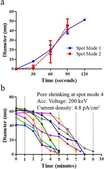
Figure 5. (a) Graphene nanopore drilling kinetics at spot modes 1 and 2 when the TEM was operated at 200 keV. Pores were drilled and expanded by converging the beam on the same area on the suspended graphene membrane. (b) Pore shrinking kinetics at spot mode 4 when the TEM was operated at 200 keV. Each line on the graph represents shrinking of an individual pore.
Download figure:
Standard image High-resolution imageShrinking of nanopores by in situ heating and electron beam irradiation has recently been reported [29, 30]. It was shown that heating graphene pores to 400–1200 °C using a thermal specimen holder inside the TEM column can result in pore shrinking (22 min to shrink a 9 nm pore) [29]. Xu et al also drew a correlation between initial pore diameter and the membrane thickness to ascertain if the pore would expand or shrink [30]. Shrinking of nanopores in multilayer graphene [7] and magnesium alloys has also been demonstrated using electron beam irradiation [31]. Our shrinking results are similar to those obtained earlier; however, we demonstrate pore shrinking in single-layer graphene, our method is faster, does not require in situ heating and provides more control over the shrinking process.
Perhaps one of the biggest advantages of our method for shrinking and fine-tuning the nanopore diameter is the ability to heal pinholes and unwanted defects without affecting the principal pore. As discussed earlier, drilling nanopores in suspended graphene often results in unwanted membrane damage (see online supplementary figure S3 for examples). Similar to pore shrinking, low-density electron beam exposure can also result in complete healing of pinholes in the graphene membrane. Our ability to heal unwanted membrane damage is demonstrated in figure 6; here peripheral pores were surgically healed and completely closed before the principal pore was size-tuned and shrunk to the desired size. For this demonstration two large pores (30–35 nm diameter, irregularly shaped and <10 nm apart) were created. In figure 6(a), the desired pore is marked with a white arrow, the large peripheral pore is marked with a black arrow and small pinholes are marked with red arrows. Although the distance between the principal pore and the peripheral pore was <10 nm, by converging the beam only on the peripheral pore (black arrow) it could be completely closed while almost maintaining the size of the principal pore (figures 6(b)–(d)). This also resulted in complete healing of the small pinholes (red arrows). After the peripheral pore was completely closed, the principal pore was also shrunk down, as seen in figures 6(e)–(h). The ability to fine tune the size of the nanopores and to heal the unwanted damage caused by the electron beam can significantly increase the usability of graphene nanopores.
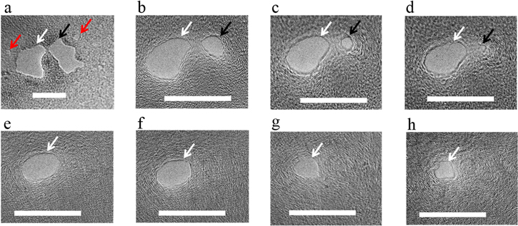
Figure 6. Surgical shrinking of pores in a graphene membrane. (a) The principal pore is marked with a white arrow, an unwanted peripheral pore is marked with a black arrow and some small pinholes are marked with red arrows. (b)–(d) A low-density electron beam was focused on the peripheral pore (black arrow) and it was fully closed along with the pinholes. (e)–(h) After the peripheral pores were closed, the electron beam was converged on the principal pore and it was shrunk down to a 6 nm pore. All scale bars: 25 nm.
Download figure:
Standard image High-resolution imageThe phenomenon of pore shrinking in graphene has been attributed to the migration of carbon adatoms from adjacent areas to the vicinity of the pore, where they combine with the unsaturated carbon atoms at the pore edge and form stable bonds [29, 30]. The adatoms or self-interstitials are the adsorbed carbon atoms occupying the position between C–C bonds and protruding out of the graphene plane. These adatoms are generally introduced in the graphene structure during growth, chemical treatment or when carbon atoms are knocked out by irradiation (pore drilling) or due to the hydrocarbon adsorbed on the sample. It is worth noting that although we were able to obtain a very clean graphene surface with our transfer recipe, a small amount of PMMA residue and adatoms could still be present and may contribute to pore shrinking. The adatoms can easily migrate along the graphene surface and combine with the unsaturated carbon atoms to facilitate self-healing (or pore shrinking in our case) or combine with other adatoms to form aggregates or hillocks [32, 33]. The activation energy required for migration of adatoms has been documented to be about 0.4 eV, making them highly mobile at elevated temperatures and during electron beam irradiation [34]. In our experiments, electron beam irradiation-induced shrinking was also accompanied by the formation of onion-like graphitic structures around the nanopore and in the shrinking zone when the membrane was irradiated for a long time (see online supplementary figure S4). The graphitic onions became more prominent with longer irradiation times [35] and we believe they are a result of adatom hillocks formed around the nanopore. In comparison with earlier works on graphene nanopore shrinking using a thermal specimen holder to heat up the whole sample [29, 30], our nanopore shrinking process is believed to be driven by the creation of a very localized thermal gradient around the converged electron beam, enabling us to surgically close the unwanted pores in the membrane.
Detection of protein translocation using graphene nanopores
Graphene nanopores have so far been used for DNA analysis, and much less attention has been given to using these devices to detect protein translocations. The motivation for using graphene nanopores for studying protein translocation is to be able to detect different conformational states of proteins, protein–protein interaction and determination of peptide sequences for single protein molecules in real time. Recently, the use of graphene nanopores for protein detection has been explored using molecular dynamics simulations [36, 37]. The authors simulated detection of different protein conformations [36] and multi-step unfolding events [37] when proteins translocate through atomically thin graphene nanopores. So far, only one report on experimental exploration of protein translocation through graphene nanopore is available and, in our opinion, the translocation data presented in the report [9] (current drop ∼50 pA, translocation time = 40 ± 20 ms for ferritin translocation at 400 mV) are not characteristic of translocations through a graphene-like thin nanopore. Protein translocation was detected after attempting to make graphene nanopores hydrophilic by coating with DPPE-PEG750 [9] and low SNR translocation data indicate insufficient pore wetting and transient protein–pore interactions. Detection of protein translocation through solid-state nanopores is believed to be more challenging than DNA translocation because of heterogeneous charge distribution, the presence of hydrophobic domains and the relatively low net surface charge density of proteins. In such cases, surface properties of nanopores play a very critical role in minimizing protein–pore interactions and facilitating smooth translocation of protein through the nanopores. The inability to reliably control the surface properties of graphene nanopores has been a major impediment in their use for studying protein translocation.
In order to evaluate the utility of our graphene nanopores, we used them to detect protein translocation and protein–protein interactions. We used antibody–antibody interaction of immunoglobulin-G (IgG) as a model system and studied interaction between Fc-specific rabbit anti-goat IgG (hereafter IgG) and an Fc fragment of goat IgG (hereafter Fc fragment) (Jackson Immuno Research, West Grove, PA, USA) using a 25 nm graphene nanopore. Such protein–protein interactions are routinely used in immunostaining methods where a primary antibody binds to a target antigen and then fluorescently tagged secondary antibodies (specific to the Fc region of the primary antibody) bind to the primary antibody, resulting in signal amplification. Before starting protein experiments, nanopore conductance was measured using 1 M KCl (pH 8, buffered with Tris-EDTA). The graphene nanopore chip was assembled in the flow cell without any pre-treatment and was used within 12 h of pore drilling. Soon after the pore had been assembled in the flow cell and flushed with KCl solution, a stable baseline was observed, characteristic of a sufficiently wet nanopore. Such pore wetting and stable conductance could not be observed when the silicon nitride surface was not coated with silicon dioxide before the graphene transfer process (data not shown). We obtained a conductance of 201.6 nS, which is in agreement with the values previously reported [38]. For translocation experiments, the antibodies were dispersed in 0.2 M KCl (at pH 5.5, buffered using acetate buffer) at a final concentration of 200 nM. IgG is a 150 kDa protein with diameter 12 nm and an isoelectric point ranging from 6.4–9.0 [39], whereas the Fc fragments are 60 kDa proteins with a diameter of around 5 nm. We chose an operating pH of 5.5 for the antibodies to have a dominant positive charge. First, only the IgG molecules were added to the cis chamber of the flow cell and a transmembrane voltage of −400 mV was applied. This resulted in a stream of antibody translocation events, with an event frequency of ∼42 events/min. Figure 7(a) (i), shows representative resistive pulses obtained during translocation of IgG molecules. Event statistics for antibody translocation events are captured in figure 7(b), which shows a current drop versus translocation time scatter plot (n = 844) along with the marginal histograms. The histograms of current drop values and translocation time were fitted with Gaussian and log-normal curves, respectively, to obtain the mean values. We observed a mean current drop value of 1420.81 pA (SD = 481.3 pA) and a mean translocation time of 121.76 μs (SD = 27.99 μs).

Figure 7. Investigation of protein–protein interaction using a graphene nanopore. (a) Current trace showing resistive pulses corresponding to individual protein translocations for Fc-specific IgG (i), Fc fragment (ii) and Fc–IgG complex. (b) Current drop and translocation time scatter plot and marginal histograms (n = 844) for IgG translocation data. A mean current drop value of 1420.81 pA (SD = 481.3 pA) and mean translocation time of 121.76 μs (SD = 27.99 μs) were obtained by fitting distribution curves to the population histograms. (c) Current drop histogram for Fc translocation events (n = 223). A mean current drop value of 446.18 pA (SD = 81.05 pA) was obtained by curve fitting. (d) Current drop histogram for Fc–IgG complex translocation events (n = 402). The bimodal distribution results from the presence of free IgG molecules and IgG molecules bound to Fc fragments. Mean current drop values of 1241.58 pA (SD = 267.53 pA) and 1989.10 pA (SD = 267.08 pA) were obtained by curve fitting. (e) Fractional current drop probability density plots for pure analytes (IgG and Fc) and protein complexes (Fc bound to IgG). The curve for Fc (blue trace) is plotted at half the probability density for better representation. All graphs and curves are color coded as free Fc (blue), free IgG (red) and Fc–IgG complex (green).
Download figure:
Standard image High-resolution image
Following the antibody translocation experiment, the flow cell was thoroughly washed and Fc fragments were introduced and detected in the similar manner. The current drop signals obtained for Fc fragment translocation events are shows in figure 7(a) (ii). Because of the small size of Fc protein (compared with the nanopore diameter), the SNR of translocation events was lower than the SNR observed for antibody translocation. As a rule of thumb, a high SNR can be obtained in nanopore experiments when 0.4dpore < danalyte < 0.8dpore; however, in the case of the Fc fragment, the diameter of the protein was only 0.24dpore, resulting in a low SNR. The current drop statistics for Fc translocation are presented in figure 7(c). Similar to the antibody data, a histogram was created for the current drop values and log-normal curve fitting was performed to obtain an average current drop value of 446.18 pA (SD = 81.05 pA). In addition to the 446.18 pA peak captured by curve fitting, there is an additional bump in the histogram around 850 pA (figure 7(c)), which can be attributed to existence of Fc dimers in the solution.
After studying the translocation behavior of individual protein components, their interaction with each other was investigated. For this experiment, Fc fragments were mixed with anti-Fc IgG in a limiting concentration (Fc:IgG 1:2) and incubated at room temperature for 2 h. After incubation, the protein complex was introduced into one of the chambers of the flow cell and translocation events were captured under similar experimental conditions. Figure 7(a) (iii) shows the characteristic signals obtained for translocation of protein–protein complexes. When the current drop data were plotted as a histogram, we observed a bimodal distribution, with one peak close to the current drop values originally observed for the pure antibody sample and a new peak shifted towards higher values (figure 7(d)). The first peak indicated the existence of free IgG molecules in the solution and the second shifted peak suggested formation of Fc–IgG complexes and an increase in the size of protein molecules. The protein–protein interaction behavior observed here is similar to interaction between HIV protein gp120 (5 nm) and anti-gp120 IgG reported earlier by our group [40]. We fitted the histogram with Gaussian mixed model to obtain the characteristic values for the two peaks. The average values obtained after curve fitting for the first and the second peaks were 1241.58 pA (SD = 267.53) and 1989.10 pA (SD = 267.08) respectively.
For low-aspect-ratio pores like the one used in this study the diameter of the molecule is much larger than the pore length and the ionic current blockades can be directly related to the cross-sectional area of the pore occupied by the translocating molecule. The magnitude of the current blockades can be estimated by the following simple relationship [41]:

where ΔI is the magnitude of the current blockades, I0 is the baseline current and dmolecule and dpore are diameters of the molecule and the nanopore, respectively. We plotted the ΔI/I0 values for the three analytes in a probability density plot, shown in figure 7(e). Considering a 25 nm pore, the right-hand side of above equation results in 0.04, 0.23 and 0.46 for a 5 nm Fc fragment, 12 nm IgG and 17 nm Fc–IgG complex, respectively. The peak values we obtained in the probability density plot agree very nicely with the theoretical values calculated based on size, except for the Fc fragment. The overestimation of ΔI/I0 values for Fc can be a result of bias towards larger current drop events because of the low SNR signal for the small protein. The clear peak separation observed in the current drop histogram and probability density curve for Fc–IgG complexes (figures 7(d) and (e) green trace), demonstrate the advantage of ultrathin graphene nanopores for distinguishing the sub-populations existing in a protein sample.
Conclusion
In summary, we demonstrate a robust way to transfer clean, defect-free and hydrophilic graphene onto nanopore chips and fabricate size-controlled nanopores in a suspended graphene membrane using electron beam-induced drilling and shrinking. Electron beam-induced shrinking was also used to heal any secondary unwanted pores, resulting in functional graphene nanopore devices. Our protein experiments demonstrate the utility of graphene nanopores for investigating single protein molecules and protein–protein interactions, which as far as we know has not been reported before. The chip preparation routine presented here improves wettability of the graphene membrane and allows for detection of complex analytes with a low charge to mass ratio.
Experimental
Graphene fabrication
The graphene layer was synthesized on the copper surface by a CVD process using RF plasma. A 300 nm thick copper film deposited on top of a silicon wafer with a 300 nm thick silicon dioxide (SiO2) layer, was inserted in an inductively coupled plasma (ICP) CVD system. After ramping up the temperature to 725 °C under Ar ambient at 50 mTorr, the sample was treated by H2 plasma with a gas flow rate of 40 sccm and RF plasma power of 50 W for 2 min. A gas mixture of Ar and C2H2 (Ar:C2H2 = 40:1 sccm), was then flowed into the chamber with 150 W RF plasma for graphene synthesis.
Experimental set-up for detection of protein translocation
The graphene nanopore chip was sandwiched between two PDMS gaskets and was assembled in a custom-built flow cell. The electrolyte filled cavities served as the cis and trans chambers. Ag/AgCl electrodes were inserted into the two electrolyte chambers and were connected to a Molecular Devices Axopatch 200B patch clamp amplifier. The current data were sampled at 200 kHz, digitized using a MD Digidata 1440 A digitizer and analyzed using pClamp 10.3 software. Recorded data were pre-conditioned for analysis by electronic low-pass Bessel filtering (10 kHz) and manual baseline correction.
Acknowledgments
This work was financially supported by the National Science Foundation Nanomanufacturing Program (CMMI 1345000) and the Korea National Research Foundation grants NRF-2015K1A4A3047100, Global Frontier (CASE-2011-0032147) and NRF-2014M3A7B6034494