Enclustra Mercury+™ XU1 SoC module: a true heavy hitter
The Xilinx® Zynq® UltraScale+™ SoC module under any circumstances
Zurich, 19th January 2018 - With the Mercury+ XU1, Enclustra presents at Embedded World 2018 in Nuremberg at booth 3-210 its fastest SoC module based on the Xilinx Zynq UltraScale+ MPSoC. It accommodates 6 ARM cores, a Mali 400MP2 GPU, up to 4 GB of extremely fast DDR4 ECC SDRAM, numerous standard interfaces, 294 user I/Os and up to 747,000 LUT4 equivalents - all on an area smaller than a credit card.

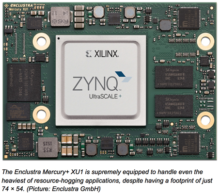
With the Mercury+ XU1, FPGA specialists Enclustra offer a quick and easy way into the Xilinx Zynq UltraScale+ MPSoC ecosystem. In addition to up to 747,000 systems logic cells across 6 ARM processors, the Mercury+ XU1 also possesses a GPU and up to 294 user I/Os. Built-in interfaces include two Gigabit Ethernet, USB 3.0 and USB 2.0, sixteen MGTs (with speeds of up to 12.5 Gbps), as well as PCIe Gen2 x4. With up to 4 GB of DDR4 SDRAM with bandwidths of 19.2 GByte/s and ECC, as well as 16 GB eMMC flash memory, the Mercury+ XU1 is supremely equipped to handle even the heaviest of resource-hogging applications, despite having a footprint of just 74 × 54 mm.
The module is available in both commercial and industrial temperature ranges, and needs just a single 5-15 V supply for operation.
Reference design and Linux at the push of a button
Enclustra offers a broad design-in support for their products. With the Mercury+ PE1-300 or Mercury+ PE1-400 baseboards, the Mercury+ XU1 can be a powerful development and prototyping platform.
Further expansion options are provided by the LPC/HPC FMC connectors on the PE1 base board, compatible with a huge range of plug-in cards from various manufacturers - ADCs, DACs, motor control cards and RF links are just a small selection of possibilities.
Enclustra also offers a comprehensive ecosystem for the XU1, offering all required hardware, software and support materials. The Mercury+ PE1 base board is a complete development platform; detailed documentation and reference designs make it easy to get started, in addition to the user manual, schema, a 3D-model, PCB footprint and differential I/O length tables.
The Enclustra Build Environment can be used to compile the Enclustra SoC modules with an integrated ARM processor very smoothly. The module and base board are selected by a graphical interface. After that, Enclustra Build Environment downloads the appropriate Bitstream, First Stage Boot Loader (FSBL) and the required source code. Finally, U-Boot, Linux and the root file system based on BusyBox are compiled.
Thanks to the family concept with compatible connectors, different types of modules can be used on the same base board. If for example, an ARM processor is not required, the Mercury+ KX2 FPGA module can be used on the same baseboard instead.
About Enclustra GmbH
Enclustra is an innovative and successful Swiss FPGA design company. With the FPGA Design Center, Enclustra provides services covering the whole range of FPGA-based system development: From high-speed hardware or HDL firmware through to embedded software, from specification and implementation through to prototype production. In the FPGA Solution Center, Enclustra develops and markets highly-integrated FPGA modules and FPGA-optimized IP cores. By specializing in forward-looking FPGA technology, and with broad application knowledge, Enclustra can offer ideal solutions at minimal expense in many areas. More information can be found at: www.enclustra.com
Download: Press kit[ZIP]
All prices subject to change. All of the information contained in this document can be changed at any time without any advance notification and is not binding for Enclustra GmbH. All trademarks are the property of their respective rights owners. Copyright © 2018 Enclustra GmbH. All rights reserved.
