How to focus light at the nanoscale
December 11, 2012

Artist’s impression of nanofocusing device (credit: Young-Hee Lee, Caltech)
California Institute of Technology (Caltech) engineers have created a device that can focus light into a point just a few nanometers (billionths of a meter) across — an achievement they say may lead to next-generation applications in computing, communications, and imaging.
The Caltech device complements IBM’s just-announced “silicon nanophotonics,” which allows for the integration of different optical components side-by-side with electrical circuits on a single silicon chip.
Focusing light into tinier spaces can squeeze more data through optical fibers and increase bandwidth, and optical devices can also be made more compact, requiring less energy to power them.
But once you reach dimensions smaller than the wavelength of light — a few hundred nanometers in the case of visible light — you reach the “diffraction limit,” and it’s physically impossible to focus the light any further.
Bypassing the diffraction limit

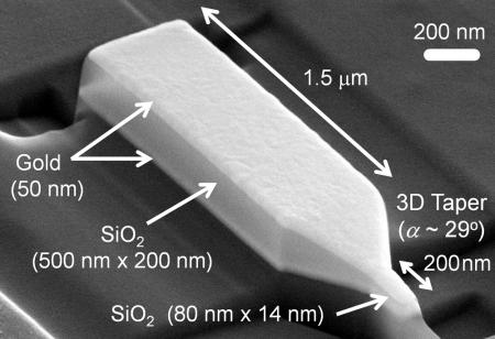
Nanofocusing device (credit: Young-Hee Lee, Caltech)
But now the Caltech researchers, co-led by assistant professor of electrical engineering Hyuck Choo, have built a new kind of waveguide — a tunnel-like device that channels light — that gets around this natural limit.
The waveguide is made of amorphous silicon dioxide (similar to glass) covered in a thin layer of gold. Just under two microns long, the device is a rectangular box that tapers to a point at one end.
As light travels through the waveguide, the photons interact with electrons at the interface between the gold and the silicon dioxide. Those electrons oscillate, and the oscillations propagate along the device as waves — similarly to how vibrations of air molecules travel as sound waves. Because the electron oscillations are directly coupled with the light, they carry the same information and properties — and they therefore serve as a proxy for the light.
Instead of focusing the light, the new device focuses these coupled electron oscillations, called surface plasmon polaritons (SPPs). The SPPs travel through the waveguide and are focused as they go through the narrow end.
The new device is built on a semiconductor chip with standard nanofabrication techniques, says Choo, so it is easy integrate with today’s technology
Previous on-chip nanofocusing devices were only able to focus light into a narrow line. They also were inefficient, typically focusing only a few percent of the incident photons, with the majority absorbed and scattered as they traveled through the devices.
With the new device, light can be focused in three dimensions, producing a point a few nanometers across, and using half of the light that’s sent through, Choo says. (Focusing the light into a slightly bigger spot, 14 by 80 nanometers in size, boosts the efficiency to 70 percent).
Applications in imaging, computing, and communication
- Efficient, high-resolution biological-imaging instrumentA biologist can dye specific molecules in a cell with fluorescent proteins that glow when struck by light. Using the new device, a scientist can focus light into the cell, causing the fluorescent proteins to shine. Because the device concentrates light into such a small point, it can create a high-resolution map of those dyed molecules. Light can also travel in the reverse direction through the nanofocuser: by collecting light through the narrow point, the device turns into a high-resolution microscope.
- Computer hard drives that hold 50 times more memoryNormal hard drives consist of rows of tiny magnets whose north and south poles lay end to end. Data is recorded by applying a magnetic field to switch the polarity of the magnets. Smaller magnets would allow more memory to be squeezed into a disc of a given size.But the polarities of smaller magnets made of current materials are unstable at room temperature, causing the magnetic poles to spontaneously flip — and for data to be lost.Instead, more stable materials can be used — but those require heat to record data. The heat makes the magnets more susceptible to polarity reversals. So to write data, a laser is needed to heat the individual magnets, allowing a surrounding magnetic field to flip their polarities.Today’s technology, however, can’t focus a laser into a beam that is narrow enough to individually heat such tiny magnets. Indeed, current lasers can only concentrate a beam to an area 300 nanometers wide, which would heat the target magnet as well as adjacent ones — possibly spoiling other recorded data.Because the new device can focus light down to such small scales, it can heat smaller magnets individually, making it possible for hard drives to pack more magnets and therefore more memory. With current technology, discs can’t hold more than 1 terabyte (1,000 gigabytes) per square inch. A nanofocusing device, Choo says, can bump that to 50 terabytes per square inch.
- Data-transfer and communication applicationsAs computing becomes increasingly reliant on optics, devices that concentrate and control data-carrying light at the nanoscale will be essential — and ubiquitous, says Choo, who is a member of the Kavli Nanoscience Institute at Caltech. “Don’t be surprised if you see a similar kind of device inside a computer you may someday buy.”
The next step is to optimize the design and to begin building imaging instruments and sensors, Choo says. The device is versatile enough that relatively simple modifications could allow it to be used for imaging, computing, or communication.
The research was funded by the Defense Advanced Research Projects Agency (DARPA) Science and Technology Surface-Enhanced Raman Spectroscopy program, the Department of Energy, and the Division of Engineering and Applied Science at Caltech.