
Understanding Schematics
If you're looking to get a better handle on how to read schematics, this helpful guide will give you a head start.
If you're looking to get a better handle on how to read schematics, this helpful guide will give you a head start.
Every new electrical circuit board design starts as an idea. That idea is then defined, with words and diagrams, in a specification. Anyone can take an idea this far, but the next step requires a fundamental understanding of circuit schematics.
Circuit schematics are the bridge between conceptual electrical design and physical realization of a printed circuit board assembly, or PCBA.

Example circuit schematic: Class A common-base small-signal high gain amplifier
Schematics have two fundamental purposes. First, they communicate design intent. To someone skilled in the art of electrical design, schematics should clearly convey the intent of the design. And second, they exist to direct and drive the PCB layout.
To get a good start on understanding schematics you should understand some basic things: component symbols, reference designators (REFDES), nets, and outputs.
Reference Designators (REFDES)
Reference designators are unique identifying labels for each physical component and they communicate a lot about the components to which they refer.
Proper REFDES use tells the schematic reader the type of component and the number of symbols per component. While there are standard symbols that represent various types of electrical components, which we will discuss next, not all schematics follow all of those standards.
In a case where every passive component is shown as a generic box with pins, reference designator prefixes can tell you a lot about the type of component that symbol represents. Reference designators also serve as the link to the bill of materials (BOM). The BOM has the part number of every component in your PCBA design, and it indicates which locations should have that part installed, by REFDES.
The industry-standard format for reference designators includes a letter code, indicating the type of component, followed by a unique number.
| BT = Battery | J = Connector | R = Resistor |
| C = Capacitor | K = Relay | S or SW = Switch |
| D = Diode | L = Inductor | T = Transformer |
| F = Fuse | P = Connector | U = Integrated Circuit |
| H = Hardware | Q = Transistor | Y = Crystal |
We will indicate the REFDES for each component as we identify their symbols below.
Component Symbols
Component symbols in a schematic represent physical components that will be soldered to the printed circuit board (PCB) during the assembly process. Sometimes they also might represent PCB structures, like vias or test points.
Component symbols are often an industry-standard shape or drawing that indicates what type of electrical components they are, though sometimes they are nothing but a rectangle with pins. Resistors, capacitors, inductors, diodes, and transistors all have standard symbols that we will cover briefly below.
Component symbols always have one or more pins to which electrical connections can be made. Each schematic symbol pin has a number that corresponds with the physical component drawing. One or more symbols may be used to define a single electrical component. Components with many pins are often represented by multiple schematic symbols simply to allow for readable schematics.
In the case of a part defined by multiple symbols, each partitioned symbol that refers to the same physical component shares the same reference designator.

Commonly used schematic symbols
Resistor
Resistors are extremely common electrical components. They are usually shown as a zigzag line in the US, though the international standard shows them as just a rectangle.
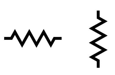
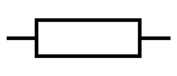
The US (top) and international (bottom) symbols for resistors
Resistors are identified in schematics with a reference designator (REFDES) starting with the letter “R”.
Capacitor
Capacitors are also very common. They are shown as two lines separated by a gap, conveying their fundamental construction of two charged plates separated by a dielectric. The two primary capacitor symbols are non-polarized and polarized.
Polarized capacitors are denoted by a curved line (to indicate a negative terminal) and/or a plus sign (to indicate a positive terminal).

Capacitor symbols. Shown are a non-polarized capacitor on the far left and three versions of a polarized capacitor.
Capacitors are identified in schematics with a reference designator (REFDES) starting with the letter “C”.
Inductor
Inductors, like resistors and capacitors, are fundamental passive components used in electric circuits. Inductors are shown as a series of curves representing their basic construction. Inductors are most simply constructed with a coil of wire around some core material.

Inductor symbol
Inductors are identified in schematics with a reference designator (REFDES) starting with the letter “L”.
Diode
Diodes are electrical components that only permit current to flow in one direction. There are a variety of diode types. Zener diodes, for example, don’t allow reverse current until the diode’s reverse voltage reaches a certain, defined level.

Diode symbol
A light-emitting diode (LED) produces light when current flows through it in the forward direction. A Schottky diode is constructed so it operates similar to a simple diode, but switches faster and has a lower forward voltage drop.

Zener diode symbol

Schottky diode symbol
Diodes are identified in schematics with a reference designator (REFDES) starting with the letter “D” or “Z” (for Zeners). “LED” is sometimes used for light-emitting diodes.
Transistor
Transistors are like electrical switches where a bias voltage or current in one area turns on the current flow across the main terminals.
There are two fundamental types of transistors: bipolar junction transistors (BJTs) and field-effect transistors (FETs).
Simplistically, BJTs are current-controlled devices where a current flowing into or out of the base pin turns on a larger current through the collector and emitter pins.

BJT symbols
Also simplistically, FETs are voltage-controlled devices, where a voltage on the gate pin turns on a current through the drain and source pins. There are a wide variety of drawings used for transistors, indicating different amounts of internal component details.
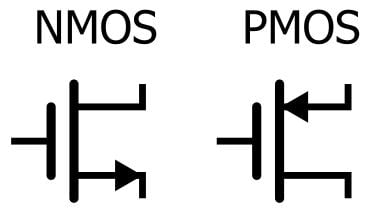
FET symbols
Transistors are identified in schematics with a reference designator (REFDES) starting with the letter “Q”. “M” is sometimes used for MOSFET devices. “T” is sometimes incorrectly used, and should be avoided.
For more detailed information on BJTs, FETs, IGBTs, and more, check out our article specifically on the schematic symbols for transistors.
Variable Resistors
Variable resistors, such as potentiometers and rheostats, are resistors that change resistance in accordance with a user’s adjustments. Two-terminal variable resistors are shown as a resistor with an arrow across it, while potentiometers (which have three terminals) add an arrow pointing at the side of the resistor symbol.

Rheostat symbol

Potentiometer symbol
Voltage-dependent resistors, or varistors, look similar to a variable resistor, but with a line across it instead of an arrow.
Varistor symbol
Special resistors are most often identified in schematics with a reference designator (REFDES) starting with the letter “R”, though “VR” (for variable resistors or potentiometers) or “RV” (for varistors) are sometimes used.
Integrated Circuit
Integrated circuits are entire electrical circuits created in semiconductor material in a single package. Integrated circuits are the processors, memory, operational amplifiers, and voltage regulators that look like squares or rectangles mounted on a printed circuit board.
Integrated circuits are shown as a box, or collection of boxes, with labeled pins for power, inputs, and outputs.

Integrated circuits are identified in schematics with a reference designator (REFDES) starting with the letter “U”, or sometimes the letters “IC”.
Crystal/Oscillator/Resonator
All three of these provide a known, steady frequency output when energized in a circuit. Crystals, oscillators, and resonators are not the same thing, having different characteristics and requiring different supporting circuitry, but their fundamental purposes are similar.

Crystal symbol
Crystals and oscillators are identified in schematics with a reference designator (REFDES) starting with the letter “Y”. “X” is occasionally used; this letter is also a catch-all for components not fitting another category.
Digital Logic Gates
There are many digital logic gates - more than can be described in detail in this overview. For a full explanation of digital logic and the many different types of logical gates, see the AAC textbook page on Digital Signals and Gates.
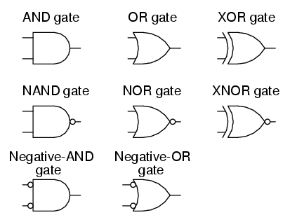
Logic gates are sold as integrated circuits, and therefore they are identified in schematics with a reference designator (REFDES) starting with the letter “U”, or sometimes “IC”, just like other integrated circuits.
Operational Amplifier
Operational amplifiers and comparators have a variety of useful functions in circuits, and they are shown as sideways triangles in schematics, with a (+) and a (-) input, and sometimes power and ground pins.

Op-amp symbol
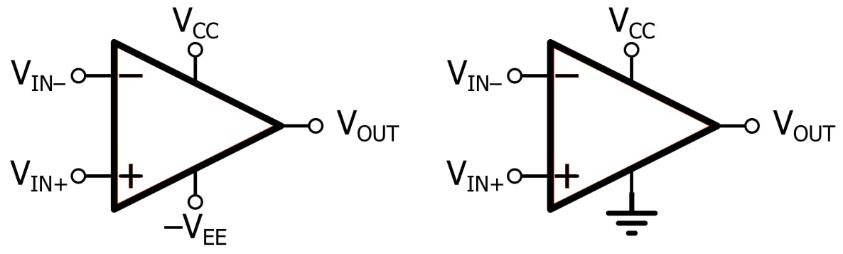
A dual-supply op-amp circuit (left) and a single-supply configuration (right) with power and ground pins indicated
Operational amplifiers and comparators are identified in schematics with reference designators (REFDES) starting with the letter “U”, or sometimes “IC”, just like other integrated circuits. Additionally, op-amps sometimes use a REFDES starting with “OP”.
Connector/Header
Connectors and headers are where other circuits or cables are connected to the circuit described by the schematic. There are a wide variety of types and orientations of connectors, and they are likewise represented in schematics by a wide variety of symbols.
Sometimes the schematic symbols are just simple rectangles, and sometimes the schematic symbols are drawings made to look like the physical connectors they represent.

Connector symbols
Connectors and headers are most often identified in schematics with a reference designator (REFDES) starting with the letter “J” or the letter “P”.
Switch
Switches are usually shown with a schematic symbol that represents the type of switch and the number of poles/throws and pins.

Switch symbols
Switches are identified in schematics with a reference designator (REFDES) starting with the letters “SW”.
Battery
Batteries are shown with a schematic symbol that has a long line and a short line, together representing one battery cell. In practice, most battery schematic symbols are drawn as two cells regardless of how many cells the battery actually contains.

Battery symbol
Batteries are identified in schematics with a reference designator (REFDES) starting with the letter “B”.
Transformer
Transformers are usually shown with a schematic symbol that symbolically represents how a transformer works. It looks like two parallel inductor coils with something in between them, usually a line or two.

Transformers are identified in schematics with a reference designator (REFDES) starting with the letter “T”.
Fuse/PTC
Fuses or PTCs (positive temperature coefficient devices) are circuit protection devices that “blow” (burn out) or increase resistance dramatically in the case of too much current flowing through them.
Fuses are usually shown in schematics with a symbol that looks like a sideways letter “S”.

Fuse symbol
Fuses are identified in schematics with a reference designator (REFDES) starting with the letter “F”.
PTCs are usually shown as a box with a line through it diagonally; the same symbol is used for PTC thermistors.

PTC symbols
PTCs are identified in schematics with a reference designator (REFDES) starting with the letter “R”, “VR”, or “PTC”.
Non-component Symbols
There are other symbols in schematics that do not represent physical components. Some symbols represent physical structures to be built into the PCB, itself, like test points or mounting holes.

Test point symbols
Other schematic symbols represent power or ground rails.

Ground symbol
Still other schematic symbols are used for interconnection between different pages of the schematic, with labels identifying what electrical net they are part of.
Non-component symbols often have no reference designators. Some will have reference designators (REFDES) starting with the letters “TP” (test points), “MH” (mounting holes), or “X” (generic catch-all for otherwise unspecified types).
For more in-depth information on several of the symbols discussed in this article, check out Robert Keim's treatment of schematic symbols for passive components.
Nets
In schematic and printed circuit board parlance, nets are the PCB-wired electrical connections. Nets appear as lines connecting component symbol pins to other pins or nets.
It is a best practice when drawing schematics to label important nets so that they can be clearly identified when laid out on a PCB design. If two nets are not drawn as connected but have the same label, they will be treated as physically connected by the schematic capture software so that when the design is exported to a PCB layout tool they will be the same net.
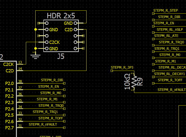
Image of a schematic with two nets not drawn connected, but labeled the same so physically connected, in this case "STEPM_R_EN"
It is a schematic capture best practice to use special symbols to show net connections to other pages, or parts of the same page, when not drawn as connected. These are intrapage (within a page) or interpage (between pages) connection symbols.

Interpage connectors
For readability, good schematics avoid overlapping nets wherever possible—but this is not always possible. When two nets connect, most schematic drawing tools add a connection dot or circle. The absence of the connection dot means the two nets are not connected, just passing over each other. More advanced schematic drawing tools show a wire hop to make it even more clear that the two nets are not connected.

Connected nets
.png)
Non-connected nets (with wire hop)
Important Outputs: Netlist and BOM
Netlist
The most important output of a schematic is the netlist. This file, or set of files, is the primary input to the PCB layout software, and it is used by layout designers to guide placing and routing for all of the circuits on a board.
Netlist formats vary, but generally they specify in a pretty simple form every component or symbol in the schematic, and every connection (net) between them. If you have named your nets in your schematic, those net names will appear in the netlist as the connection point between parts. If you did not name a net, the netlist output tool will generate a name for it.
Typically, a netlist will contain multiple tables: one listing the parts and their names, one listing the net names and their connections, etc. Netlists can also be used to include additional information necessary for SPICE circuit simulations. See some simple example netlist outputs here.
BOM (Bill of Materials)
The other important output of a schematic is a bill of materials or BOM. The BOM output is a spreadsheet or database that matches every REFDES in the schematic with a physical component and a part number.
There are a variety of formats for the BOM output, depending on how sophisticated your schematic and parts database are, and what kind of output you want. At the simplest end of the spectrum, you may have a list of reference designators, each with a manufacturer’s part number.

Screenshot of an OrCAD BOM output
More complex BOMs will include your company’s internal part numbers, quantities of a part used in multiple places, multiple vendor part numbers that can be used for a given part, etc. The BOM contains the information necessary to take a schematic and actually build it into an assembly.
There is much more to schematics than just these key things. Entire industries and careers are built around schematic design and PCB assembly. But understanding these five things will put you well on your way to understanding the most important fundamentals of schematics.
Are you looking at a schematic and need help with something not covered in this article? Tell us about it in the comments and we may put together an article to help!


Simple, informative article with clear information. Good work. Thanks, Matthew.
Matthew, You are putting out a tremendous amount of misinformation. Suggest you read over: ANSI/ASME Y14.44 concerning reference designations; IEEE 315, Clause 22.4 for the list of class letters to be used in forming a REF DES; IEC 60617 for the proper graphic symbol to use (most of these are found in IEEE 315A); and NIST Special Publication 811 on proper SI presentation. All people doing schematic capture or reading an electrical/electronic schematic diagram should have access to these “standards”.
—Regards, Larry